“Know how to solve every problem that has been solved.”“What I cannot create, I do not understand.”— Richard Feynman
Thermal Oxidation: The Deal-Grove Model
Semiconductors
⛓
What you need to know first
2 concepts, 1 layers
The requisite-knowledge inventory for this page, bottom-up: the
primitives at the base, combined upward until you reach what this page
assumes. Skim the layers you already own; start wherever the ground gets unfamiliar.
base
Arrhenius rate lawsconcept
The diffusion equationconcept
↳you are here
2 of these are concepts without a dedicated page yet —
the grey chips. Following the linked ones first makes the rest land.
Silicon did not win the semiconductor industry because it is the best
semiconductor — germanium has higher mobility, and several III-V compounds
beat it on almost every electronic figure of merit. Silicon won because of
what happens when you heat it in oxygen: it grows its own insulator, a
dense, adherent, electrically superb film of SiO2, in a furnace,
with no deposition step at all. Every gate oxide, every masking layer,
every isolation region in seventy years of devices started as this
reaction. This page is the first stop on the site's
from sand to transistor arc: grow the oxide, then
dope through its openings,
then measure the junction you
made, then draw the
openings in the first place.
One ODE: diffuse through, react at the bottom
Deal and Grove (J. Appl. Phys. 36, 3770 (1965)) reduced oxidation
to a supply chain with two bottlenecks in series. Oxidant arrives at the
oxide surface, diffuses through the oxide already grown, and
reacts at the buried Si/SiO2 interface — the oxide grows from
the bottom, not the top. In steady state the two fluxes match, and the
growth rate is
dtdx=2x+AB,
whose integral is the famous linear-parabolic law
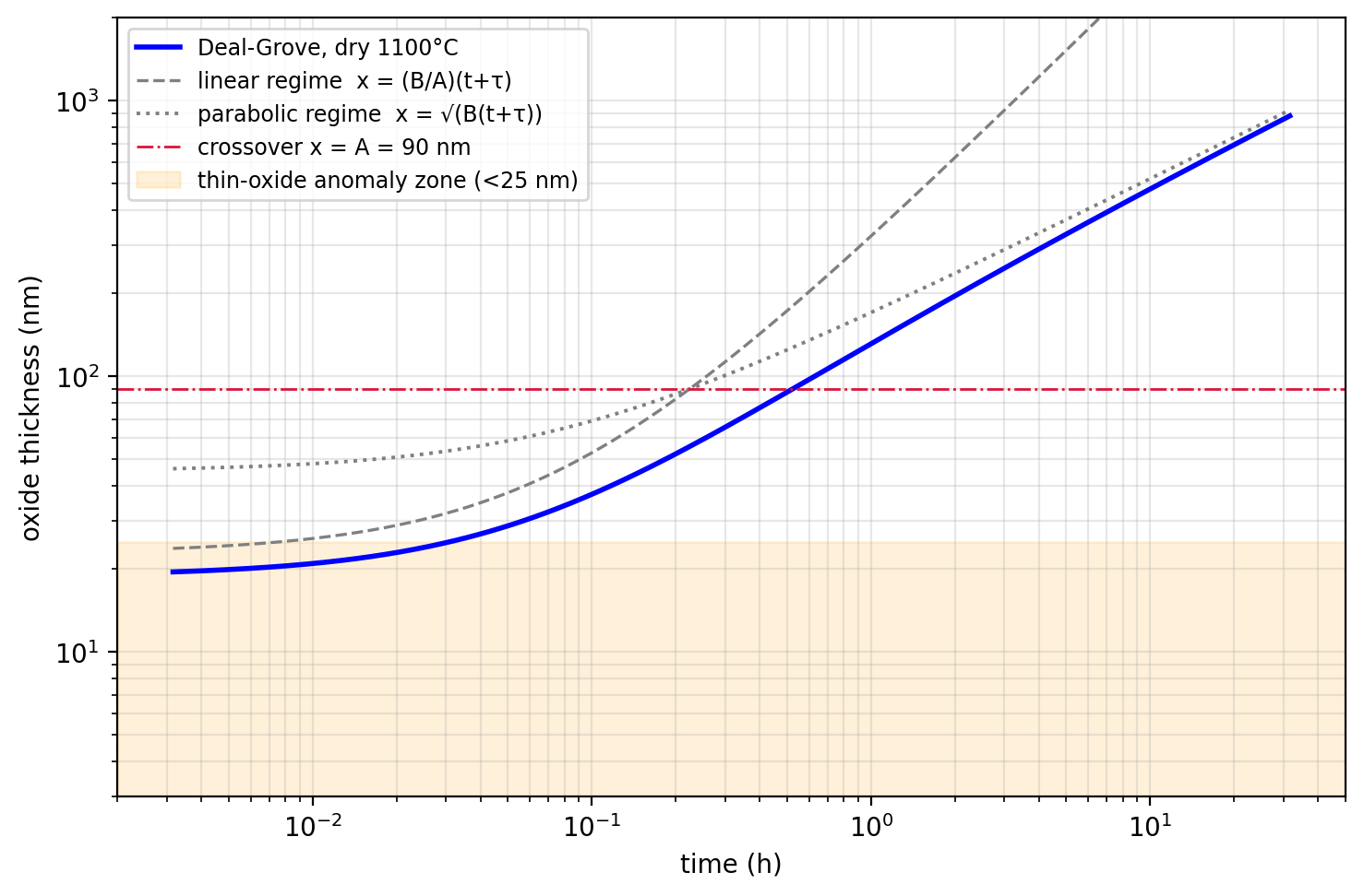
x2+Ax=B(t+τ). Two regimes fall out. While the film
is thin (x≪A), diffusion is easy and the interface
reaction is the bottleneck: growth is linear at rate B/A.
Once the film is thick, the oxidant's slog through the oxide dominates:
growth is parabolic with constant B, and each nanometer costs
more time than the last. The crossover sits exactly at
x=A.
def dg_closed(t, A, B, tau): """Deal-Grove closed form: x^2 + A x = B (t + tau).""" return 0.5 * A * (np.sqrt(1 + 4 * B * (t + tau) / A**2) - 1)def dg_ode(t_grid, A, B, tau): """Or integrate the physics directly: dx/dt = B / (2x + A).""" x = dg_closed(0.0, A, B, tau) out = [x] for t0, t1 in zip(t_grid[:-1], t_grid[1:]): h = t1 - t0 f = lambda xx: B / (2 * xx + A) # RK4 k1 = f(x); k2 = f(x + 0.5*h*k1); k3 = f(x + 0.5*h*k2); k4 = f(x + h*k3) x = x + h / 6 * (k1 + 2*k2 + 2*k3 + k4) out.append(x) return np.array(out)
Using Deal and Grove's own published (111) rate constants at 1100°C
(dry O2: A=0.090μm,
B=0.027μm2/h,
τ=0.076h):
Deal-Grove, dry O2, 1100 C, (111) Si  [A = 0.090 um, B = 0.027 um^2/h]:
  closed form vs RK4 ODE: max |diff| = 1.05e-11 um
  x(1 h) = 131.3 nm   x(10 h) = 478.5 nm
  crossover x = A = 90 nm at t+tau = A^2/B = 0.30 h
  tau = 0.076 h encodes an 'initial' oxide of 18.9 nm — the thin-oxide fudge
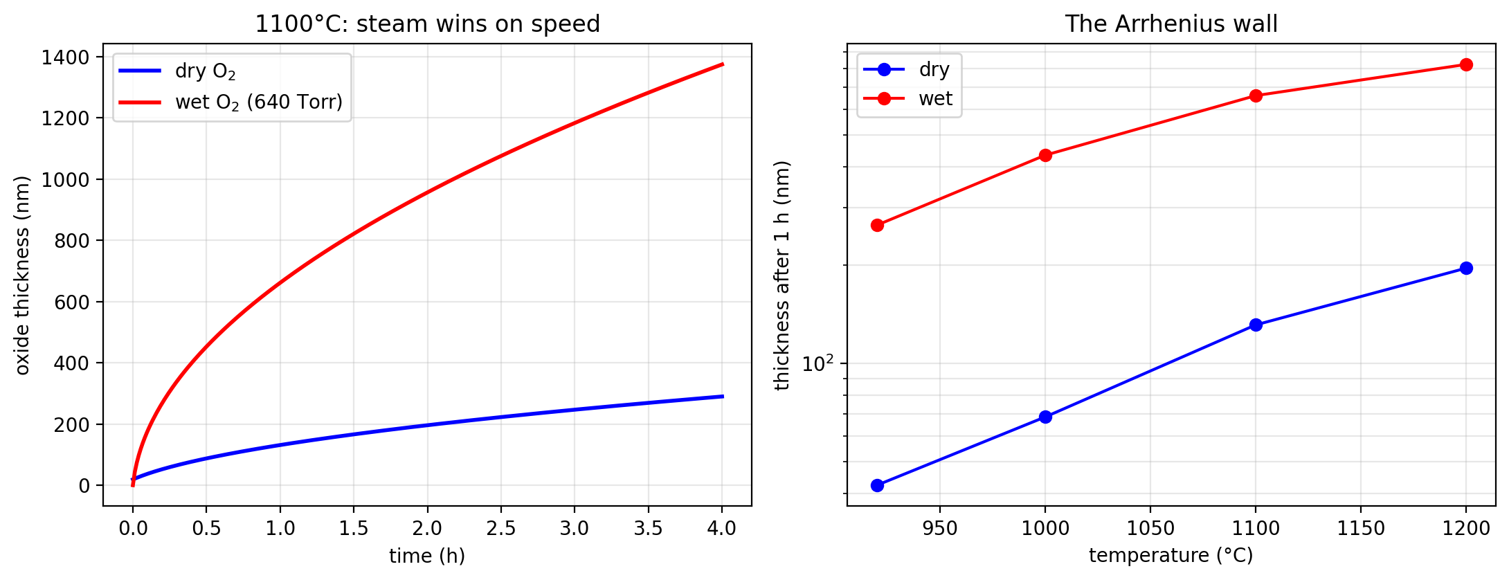
  wet 1100 C, 1 h: 661 nm vs dry 131.3 nm (5x)
  Si consumed / oxide grown = (rho_ox/M_ox)/(rho_si/M_si) = 0.443
An hour buys 131 nm; ten hours buy only 479 — the parabolic regime
punishing impatience with a square root. Note the closed form and the
direct RK4 integration of dx/dt agree to
10-11 µm: the algebra and the physics are the same statement.
Wet versus dry: the speed-quality trade
Steam oxidizes five times faster at the same temperature — water is
smaller than O2 and far more soluble in the oxide, so the
parabolic constant jumps twenty-fold. The price is a slightly looser,
wetter film with more interface traps. Fabs use both accordingly: thick
field and masking oxides grown wet, where microns matter and quality
doesn't; thin gate oxides grown dry, where every interface state is a
threshold-voltage error. The right panel is the other lever — both rate
constants are Arrhenius in temperature, so a 100°C change moves an hour's
growth by factors, which is why furnace temperature control is a
tenth-of-a-degree business.
The model's own confession: τ and the thin-oxide anomaly
Deal and Grove needed the offset τ to fit their dry data —
equivalent to pretending every wafer starts with 18.9 nm of oxide already
grown. That is the model confessing where it fails: below roughly 25 nm,
dry oxidation runs faster than the linear-parabolic law predicts,
for reasons the model's serial-bottleneck picture cannot produce
(Massoud's correction adds an exponential rate-enhancement term; the
microscopic mechanism was argued about for decades). The fudge was benign
in 1965. It stopped being benign when gate oxides became 2-5 nm
thick — the entire film living inside the anomaly zone — and modern
ultrathin-oxide recipes are calibrated empirically rather than trusted to
Deal-Grove. A model plus the region where it lies is worth more than a
model alone.
The oxide eats the wafer
The silicon in SiO2 has to come from somewhere: the wafer.
From densities and molar masses,
(ρox/Mox)/(ρSi/MSi)=0.443 — growing
100 nm of oxide consumes 44 nm of silicon, so the interface retreats
into the wafer while the surface rises above it. Process
engineers exploit this constantly: an oxide grown and then stripped
leaves a recessed, atomically fresh silicon surface, and the consumed
thickness is a built-in depth gauge.
Try First
Each prompt asks a checkable question about the working code or math
above — predict an output, derive a sign, state an invariant, find a
bug. Commit to an answer before clicking "reveal." That commitment is
the whole point: if your answer matched, you understand the piece you
were looking at; if it didn't, that's the part worth re-reading.
predict
You have grown oxide for time t and want more, so you run
for time t again. How much extra thickness do you get in
the linear regime? In the parabolic regime?
answer
Linear: the same again — thickness doubles. Parabolic:
x∝t, so doubling the time multiplies the
thickness by 2 — only 41% more, because the new
oxidant must cross everything you already grew. In the run above,
hours 2 through 10 add barely 2.5 times what the first hour did.
Every furnace schedule in a fab is built around this diminishing
return.
why does this work
The oxide grows at the buried Si/SiO₂ interface, not at the outer
surface. Why is that a gift for device quality?
answer
The electrically active interface — where the transistor channel will
live — is continuously regenerated inside the crystal, below
any surface contamination. Dirt, adsorbates, and handling damage stay
on the outer surface and get buried in inert oxide; the fresh
interface never saw the room. A deposited insulator has exactly the
opposite property: its critical interface is the one exposed to the
world just before deposition. This, as much as the oxide's bulk
quality, is why silicon's native oxide was unbeatable.
what if
The constants quoted are for (111)-oriented silicon; (100) wafers —
the ones actually used for MOSFETs — oxidize noticeably slower in the
linear regime but identically in the parabolic regime. What does that
tell you about the two constants?
answer
The linear constant B/A contains the interface reaction, which
depends on how many silicon bonds per unit area present themselves
to the oxidant — a crystal-orientation property ((111) is denser in
available bonds). The parabolic constant B is pure diffusion through
amorphous SiO₂, which has no memory of the crystal beneath. One
experiment, two constants cleanly attributed to two mechanisms —
the kind of factorization that makes a model trustworthy.
Reproduce it
scripts/gen_semiconductors.py generates every number and
figure on this page and its two siblings in seconds. Next on the arc:
with oxide windows in place, push dopants through them —
dopant diffusion.