“Know how to solve every problem that has been solved.”“What I cannot create, I do not understand.”— Richard Feynman
Dopant Diffusion: Two Profiles, One Fick's Law
Semiconductors
⛓
What you need to know first
3 concepts, 2 layers
The requisite-knowledge inventory for this page, bottom-up: the
primitives at the base, combined upward until you reach what this page
assumes. Skim the layers you already own; start wherever the ground gets unfamiliar.
2 of these are concepts without a dedicated page yet —
the grey chips. Following the linked ones first makes the rest land.
A transistor is a pattern of where the dopants are. Getting them
there is diffusion — atoms of boron or phosphorus hopping between lattice
sites at 1000 °C — and the whole design space is two boundary conditions on
one equation. Hold the surface at a fixed concentration and dopant floods in
as a complementary error function; seal the surface and let a fixed dose
spread and it relaxes into a Gaussian. Fabs run them in sequence:
predeposition to meter in a precise dose, then a
drive-in to push it to depth and set the junction. This
page runs Fick's second law as fifteen lines of finite differences,
recovers both closed forms to five digits, and — the part worth staying
for — uses the one quantity the numerical scheme must conserve to catch a
bug that the eye would have called physics.
def fd_diffuse(C0, dx, D_of_C, t_total, bc_surface=None):
    """Explicit finite differences for dC/dt = d/dx( D(C) dC/dx ).
    bc_surface = fixed surface value (predep) or None (conservative, drive-in)."""
    C = C0.copy()
    Dmax = D_of_C(np.array([C.max() or bc_surface])).max()
    dt = 0.4 * dx * dx / Dmax                       # explicit stability bound
    nsteps = int(t_total / dt) + 1
    dt = t_total / nsteps
    for _ in range(nsteps):
        D_half = 0.5 * (D_of_C(C)[1:] + D_of_C(C)[:-1])   # diffusivity on edges
        flux   = D_half * (C[1:] - C[:-1]) / dx           # Fick flux between nodes
        C[1:-1] += dt / dx * (flux[1:] - flux[:-1])       # divergence of flux
        if bc_surface is not None:
            C[0] = bc_surface                             # constant source
        else:
            C[0] += dt / dx * flux[0]                     # zero-flux: dose conserved
        C[-1] = 0.0
    return C
One ruler: √(Dt)
Every length in diffusion is measured by Dt, and
D is Arrhenius — D=D0e−Ea/kT — so it is
savagely temperature-sensitive. For boron, the same 150 °C that separates
the predep from the drive-in changes D by a factor of 36:
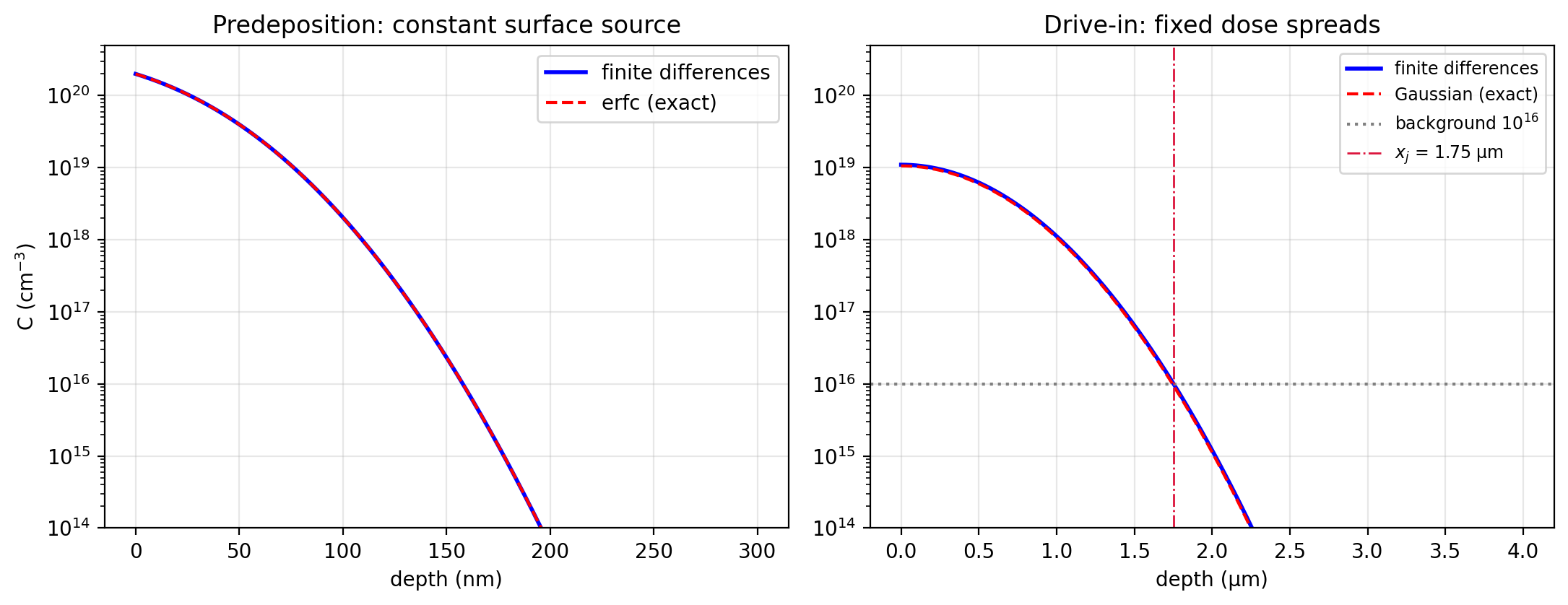
Boron diffusion  [D0 = 0.76 cm^2/s, Ea = 3.46 eV, Plummer Table 7-5]:
  D(950 C) = 4.207e-15 cm^2/s   D(1100 C) = 1.518e-13 cm^2/s
  predep 30 min:  sqrt(Dt) = 27.5 nm   dose Q = 6.210e+14 cm^-2
  drive-in 2 h:   sqrt(Dt) = 331 nm   (ratio 12.0 — Gaussian limit OK)
  drive-in surface conc = 1.060e+19 cm^-3
  junction depth x_j (C = 1e+16 background) = 1.75 um
  FD predep vs erfc: max error = 4.44e-06 of Cs;  dose FD = 6.210e+14 (-0.00%)
  FD drive-in vs Gaussian: max deviation = 3.82% of peak
  dose conserved through drive-in to -3.33e-14%
  x_j from FD profile = 1.75 um (analytic 1.75 um)
Predeposition holds the surface at solid solubility and
lets dopant in: the profile is C(x)=Cserfc(x/2Dt),
and the total dose Q=2CsDt/π is what you are
actually buying — 6.2×10¹⁴ cm⁻² here, metered by time and temperature. The
finite-difference solver tracks the exact erfc to 4×10⁻⁶ of the surface
value, and returns that dose to the last digit.
Drive-in then seals the surface (the source is gone) and
lets that fixed dose redistribute: C(x)=(Q/πDt)e−x2/4Dt,
a Gaussian whose peak falls as it deepens because the area under
it is conserved. The drive-in Dt is twelve times the
predep's, which is exactly the regime (thin initial layer, long spread)
where the Gaussian's delta-function idealization of the starting profile is
a good approximation — and the 3.8% peak deviation the solver reports is the
Gaussian being wrong about the near-surface, not the finite differences.
The invariant catches the bug
Drive-in conserves dose exactly — no atoms enter or leave a sealed surface —
so ∫Cdx is an invariant the scheme must respect, and the
solver above holds it to 3×10⁻¹⁴, machine zero. That guarantee is also a
trap. The first version of this check measured the dose with
np.trapz and reported the drive-in gaining 4% of its
dopant — physically impossible, and alarming enough to look like a real
flux-boundary bug. It was not. trapz half-weights the surface
node, and the initial predep profile is a sharp spike right at that node, so
the trapezoidal rule mis-measured the starting dose; the fix was to compare
like with like — the solver's own conserved quantity is the discrete sum
∑CiΔx, not a trapezoidal integral of it. The
lesson is the general one for conservative schemes: measure the
invariant with the same quadrature the scheme uses to enforce it, or
you will attribute your integration rule's error to the physics.
Where the junction lands
The metallurgical junction is where the diffused dopant crosses the
background doping of the opposite type — boron (acceptor) falling past the
1016 cm⁻³ phosphorus already in the wafer. Set the Gaussian
equal to NB and solve for depth:
xj=2DtlnNBCs=1.75μm
and the junction read straight off the numerical profile agrees to the two
digits printed. The logarithm is the useful shape of it: junction depth is
dominated by Dt and only weakly (as a square root of a
log) by how much dopant you started with. To move a junction you move the
thermal budget, not the dose — which is the entire next section.
High concentration diffuses faster
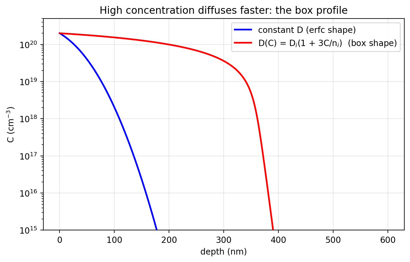
Constant D is a convenient fiction. At the concentrations real
source/drain regions reach — above the intrinsic carrier density at
temperature — the diffusivity depends on the local concentration, because
the charged point defects that carry dopant atoms scale with the Fermi
level. Model it crudely as D(C)=Di(1+βC/ni) and the
profile stops looking like an erfc: the high-concentration region diffuses
fast and flattens into a plateau, then drops through a steep box
front where D collapses. The measured front sits at 361 nm
against 109 nm for the constant-D erfc — more than three times
deeper, with an abrupt edge instead of a gentle tail. That abruptness is a
feature: sharp, box-like source/drain profiles are what shallow, low-
resistance junctions want, and they come for free from the nonlinearity.
The only code change was passing a function D(C) instead of a
constant — the solver was written to take diffusivity on the cell edges for
exactly this reason.
The thermal budget is the real currency
Because Dt is the only ruler, every high-temperature
step a wafer sees adds to the smearing of every dopant already
placed — the budgets accumulate as ∑Diti. That is the
tyranny modern processing fights:
thermal budgets sqrt(Dt):
  950 C, 30 min                sqrt(Dt) =    27.5 nm
  1100 C, 2 h                  sqrt(Dt) =   330.6 nm
  1050 C, 10 s (RTA spike)     sqrt(Dt) =     7.1 nm
A 30-minute predep at 950 °C spreads dopant 27 nm; a 2-hour drive-in at
1100 °C spreads it 330 nm. But a rapid thermal spike — 1050 °C for ten
seconds — moves it only 7 nm, while still delivering enough thermal energy
to activate the dopant and repair implant damage. That gap is why the
industry abandoned furnace drive-ins for shallow junctions and went to RTA,
then spike, then flash and laser anneals measured in milliseconds: the goal
is always maximum activation for minimum Dt. Sub-10-nm
junctions simply cannot survive a furnace. The competition between placing
dopant and not smearing it is the constraint that shapes the entire
back-end thermal sequence.
Try First
Each prompt asks a checkable question about the working code or math
above — predict an output, derive a sign, state an invariant, find a
bug. Commit to an answer before clicking "reveal." That commitment is
the whole point: if your answer matched, you understand the piece you
were looking at; if it didn't, that's the part worth re-reading.
predict
A drive-in for time t puts the junction at depth
xj. You need it 40% deeper. Do you double the time, or is
that overkill?
answer
Overkill, and then some. Junction depth scales as
Dt (the log factor barely moves), so depth goes as
t: to get 40% deeper you need
1.42≈2× the time — so doubling the time is
about right for 40%, not for 100%. The square-root ruler means late
diffusion is expensive in depth: the first minutes place most of the
junction, and each additional micron of depth costs quadratically more
thermal budget. This is the same diminishing return that governs
oxide growth in its
parabolic regime — both are Dt physics.
why does this work
Why run predeposition and drive-in as two separate steps at all? Why not
just hold the surface at solid solubility for the whole time and let the
erfc deepen?
answer
Because you would lose control of the dose. A constant-source erfc keeps
pumping dopant in for the entire duration, so the total dose grows as
t and is pinned to the (temperature-dependent) solid
solubility — you cannot choose it independently of depth. Splitting the
steps decouples the two knobs: the short predep meters the dose
(a clean Q=2CsDt/π), then the sealed drive-in
places it in depth at fixed dose. Two boundary conditions, two
independent design parameters. Modern flows replace predep with ion
implantation for even tighter dose control, but the drive-in Gaussian
is the same math either way.
what if
The solver picks its timestep as Δt=0.4Δx2/Dmax.
What breaks if you make Δx half as large to resolve a
sharp profile — and why does the Dmax matter for the
nonlinear D(C) run specifically?
answer
Halving Δx quarters the stable timestep — explicit
diffusion has a Δt∝Δx2 stability
limit (the CFL condition for parabolic equations), so four times finer
in time for two times finer in space: the cost of an explicit scheme on
a sharp front. And for the D(C) box profile, the diffusivity
is largest where the concentration is highest, so the stability bound
must use the maximumD the run will ever see, not
the initial one — bound it with the surface value or the scheme goes
unstable exactly at the high-concentration plateau it was meant to
capture. An implicit scheme (Crank–Nicolson) removes the timestep
limit at the cost of a tridiagonal solve per step — the standard trade
the moment profiles get stiff.
Extensions
Ion implantation — the modern replacement for predep: a Gaussian (Pearson-IV, really) profile placed at a chosen depth by beam energy, dose set by beam current × time. The drive-in that follows is the same Fick's-law relaxation this page solves.
Transient enhanced diffusion (TED) — implant damage creates a burst of point defects that make dopant diffuse anomalously fast during the first seconds of anneal; the single biggest reason shallow-junction modeling is hard, and the reason flash/laser anneals exist.
Implicit time-stepping — Crank–Nicolson trades the explicit Δt∝Δx2 limit for a tridiagonal solve, worth it once profiles are stiff; connects to the parabolic-PDE methods elsewhere on the site.
Where the dopants go next — the profile this page places, crossing the background doping, is the junction analyzed in the PN junction page; the openings it diffuses through were drawn by photolithography and masked by thermal oxide.
Reproduce it
scripts/gen_semiconductors.py uses Plummer's published boron
constants (Table 7-5) and validates the finite-difference solver against
both closed forms before trusting it on the nonlinear D(C) case
the closed forms cannot reach. The dose-conservation story above is real and
lives in the source comments — a standing reminder that in a conservative
scheme, the invariant is both your best test and your easiest way to fool
yourself.