“Know how to solve every problem that has been solved.”“What I cannot create, I do not understand.”— Richard Feynman
The PN Junction: From Cartoon to Poisson and Back
Semiconductors
⛓
What you need to know first
5 concepts, 3 layers
The requisite-knowledge inventory for this page, bottom-up: the
primitives at the base, combined upward until you reach what this page
assumes. Skim the layers you already own; start wherever the ground gets unfamiliar.
3 of these are concepts without a dedicated page yet —
the grey chips. Following the linked ones first makes the rest land.
Put p-type silicon against n-type and electrons pour across the boundary
into the holes, leaving behind a wall of stripped, immobile dopant ions —
a region swept clean of carriers whose fixed charge builds a field that
stops the flow. That is the depletion region, and the textbook picture of
it is a cartoon so useful it survived seventy years: a sharp box of charge,
empty inside, quasineutral outside. This page holds the cartoon up against
the real thing — a full nonlinear Poisson solve with Boltzmann carriers —
and finds it 0.8% right on the number it exists to predict. Then it does
the move that makes device physics a measurement science rather than a
story: put a known doping into a simulated capacitance–voltage
experiment and read that same doping back out of the slope. The
loop closes to 1%.
The cartoon, and why it works
The depletion approximation makes one brutal assumption — the transition
from full depletion to full neutrality is a step — and buys closed forms
for everything. The built-in potential is the difference in Fermi levels the
two dopings arrived with,
Vbi=qkTlnni2NaNd=0.835V,
and setting the integrated charge to zero across a box of width
W gives W=2εVbi(Na+Nd)/qNaNd.
For this junction — Na=1018 against
Nd=1016, a hundred-to-one one-sided junction — that is
330 nm, and it is nearly all on the lightly doped n side: 327 nm of
the 330, versus 3.3 nm on the p side. Charge neutrality forces it —
Naxp=Ndxn — so the side with less doping must deplete
wider to expose the same total charge. This is why the lightly doped side
of a junction is where all the action (and all the breakdown voltage) lives.
The junction, actually solved
def solve_poisson(Vr=0.0, psi0=None):
    """Damped Newton on 1D nonlinear Poisson: psi'' = -rho(psi)/eps,
    Boltzmann majority carriers, reverse bias Vr on the n side."""
    psi = psi0.copy() if psi0 is not None else initial_guess()
    psi[0], psi[-1] = psi_p, psi_n                 # Dirichlet: bulk potentials
    for it in range(400):
        n, p = carriers(psi, Vr)                   # ni*exp(+-psi/Vt), by side
        rho  = q * (p - n + Nnet)                  # Nnet = Nd - Na, doping
        F        = laplacian(psi) + rho / eps      # residual, zero at solution
        # Jacobian is tridiagonal: d rho / d psi = -q (p + n) / Vt
        diag = -2 / h**2 - q * (p + n) / (eps * Vt)
        dpsi = solve_tridiagonal(diag, 1/h**2, -F)
        psi[1:-1] += np.clip(dpsi, -2*Vt, 2*Vt)    # damp the Newton step
        if np.abs(dpsi).max() < 1e-10: break
    return psi, it
The real electrostatics is one nonlinear ODE:
ψ′′=−ρ(ψ)/ε, where the charge density
ρ depends on the potential through the Boltzmann carrier
statistics n,p∝e±ψ/Vt. Nonlinear because the
carriers respond to the field they create; solved by Newton's method, which
for this equation has a tridiagonal Jacobian and converges — with a little
damping on the step — in 16 iterations.
PN junction  [Na = 1e18, Nd = 1e16, ni = 9.65e9 cm^-3 (Sze & Ng 3rd ed.), 300 K]:
  Vbi = 0.835 V
  W(0) = 330 nm   (n-side 327 nm, p-side 3.3 nm)
  Poisson solver: converged in 16 Newton steps
  numeric W (half-max charge) = 333 nm vs depletion approx 330 nm (+0.8%)
  numeric W (5% threshold)    = 453 nm — the Debye tail the sharp-edge picture ignores
  numeric built-in potential = 0.835 V vs formula 0.835 V
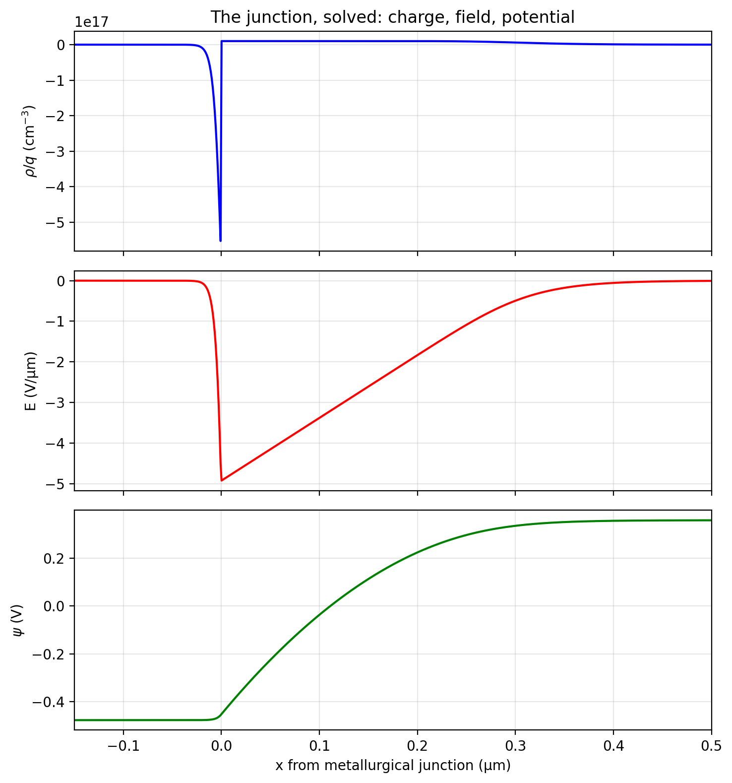
The three panels are the depletion region as it really is: charge, its
integral the triangular field, and its integral the S-shaped
potential rising by exactly Vbi. Two numbers score the
cartoon. Measured at half-maximum charge, the depletion width is 333 nm
against the approximation's 330 — 0.8% high, a genuinely good cartoon. But
measured where the charge falls to 5% of its peak, it is 453 nm: the box
has soft edges. Those edges are Debye tails — the carrier density
cannot switch on in zero distance, it relaxes over a Debye length — and they
are precisely what the sharp-box picture throws away. The built-in potential
the solver develops, with no Vbi put in anywhere, is 0.835 V
to three digits: the same number the Fermi-level formula gives, now emerging
from the electrostatics that formula summarizes.
Reading the doping back out
Here is where simulation earns its keep. A reverse-biased junction is a
capacitor whose plates are the depletion edges; widen the depletion by
pulling V more negative and the capacitance drops. The
depletion-approximation algebra predicts that 1/C2 is
linear in bias, with a slope set by the doping and an intercept at
Vbi:
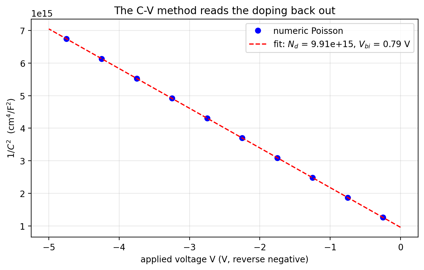
This is the whole closure. The capacitance came from differencing the
depletion charge in the numeric Poisson solution across a bias
sweep — a simulated C–V measurement, blind to the doping that was set — and
the slope returns Nd=9.9×10¹⁵ against the
1016 that went in. One percent. The input became a profile,
the profile became a capacitance curve, and the curve gave the input back:
exactly what a metrology engineer does to a real wafer, run in reverse to
validate the physics. The intercept is the honest wrinkle worth keeping —
it reads Vbi=0.792 V, about 0.04 V (roughly
2kT/q) below the true 0.835. That gap is not solver error; it is
the known majority-carrier correction the depletion-approximation C–V
formula omits, the same Debye tail that softened the box edges now showing
up in the extrapolated intercept. The doping — the thing you actually want —
comes from the slope and is immune to it, which is why C–V profiling
trusts slopes and treats the intercept as a rough guide.
Forward bias: sixty millivolts a decade
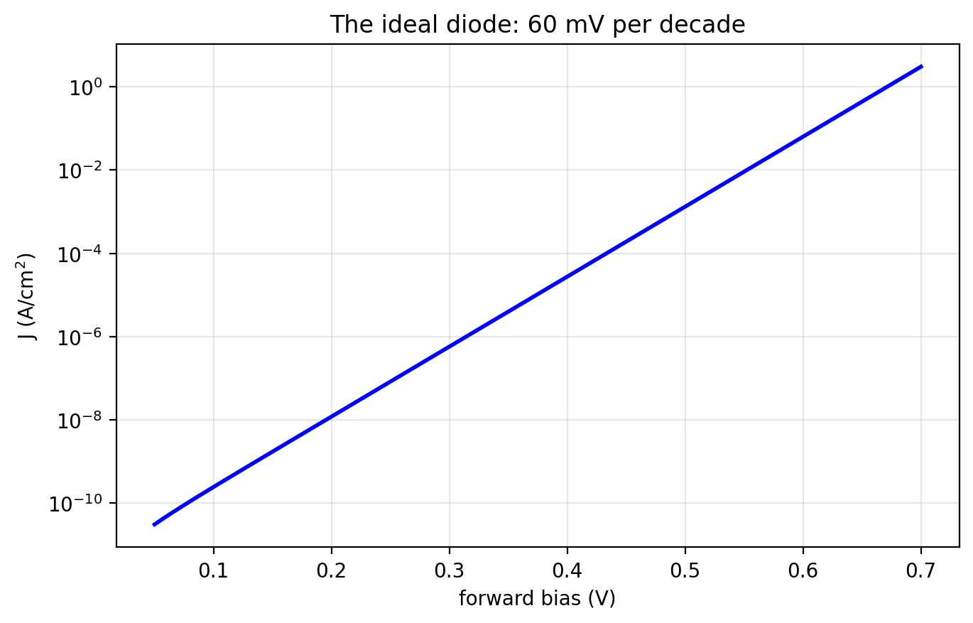
Forward-bias the junction and the current is Shockley's law,
J=J0(eV/Vt−1), with a saturation current
J0=5.3×10⁻¹² A/cm² set by minority-carrier diffusion.
On a log axis it is a straight line whose slope is the number every circuit
designer carries: 2.303kT/q=59.5 mV per decade of current —
measured here at 59.2. That 60 mV/decade is the thermodynamic speed limit on
how sharply a diode (or a transistor's subthreshold) can turn on at room
temperature, because it comes straight from the Boltzmann factor
eV/Vt. It is the reason low-power transistor scaling is hard
and the reason "subthreshold swing" is a headline device metric —
kT/q does not care about your process node.
The junction the diffusion made
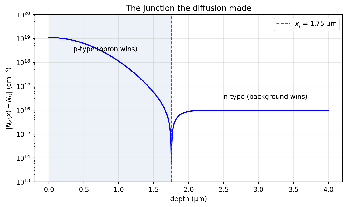
This junction did not come from nowhere. The p-side doping is exactly the
boron profile driven in on the dopant
diffusion page, crossing the wafer's 1016 background at
the 1.75 µm junction depth computed there. Oxide grown, window opened,
dopant driven, junction formed, junction measured — the four pages are one
process flow, and every number on this page traces back to a published
constant through code you can rerun. The device is where the whole arc was
headed: this is the diode, and two of them back to back with a shared middle
region is the bipolar transistor; a gate over an inverted channel between
two of these is the MOSFET the computer
architecture section is built out of.
Try First
Each prompt asks a checkable question about the working code or math
above — predict an output, derive a sign, state an invariant, find a
bug. Commit to an answer before clicking "reveal." That commitment is
the whole point: if your answer matched, you understand the piece you
were looking at; if it didn't, that's the part worth re-reading.
predict
The depletion region sat 327 nm on the n side and 3.3 nm on the p side —
a 100:1 split for a 100:1 doping ratio. Predict: reverse-bias the junction
to widen W by 3×. Does the split ratio change?
answer
No — the ratio is locked by charge neutrality, not by bias.
Naxp=Ndxn must hold at every bias (the exposed
charge on the two sides is equal and opposite), so
xn/xp=Na/Nd=100 always. Widening W by 3×
widens both sides by 3×; essentially all of the new depletion still
opens up on the lightly doped n side. This is exactly why the
lightly doped side sets the breakdown voltage: it absorbs almost the
entire depletion width, so it is where the field integrates out to the
largest voltage before avalanche. Power devices are built by making one
side very lightly doped and very wide for precisely this reason.
why does this work
The C–V intercept was off by 2kT/q, but the doping from the
slope was dead on. Why is the slope trustworthy when the intercept is not?
answer
Because the error is an additive offset in Vbi,
and the slope of 1/C2 versus V doesn't see
additive offsets in the intercept. The majority-carrier tails at the
depletion edge effectively shift where the "edge" is by a fixed
∼kT/q of potential — the same at every bias — so they
translate the whole 1/C2 line up or down without tilting
it. The doping lives in the tilt (d(1/C2)/dV∝1/Nd),
which is untouched; the built-in potential lives in the intercept, which
is shifted. A measurement's robustness is a question of which
parameter carries the answer — put your answer in the slope, not
the intercept, whenever the systematic error is a constant offset.
what if
The Newton step is clipped to ±2Vt per iteration. Drop the
clip and the solver diverges on the first step. Why does undamped Newton
blow up on this particular equation?
answer
Because the nonlinearity is exponential. The carrier densities go as
eψ/Vt, so a Newton step that overshoots the potential
by even a few Vt exponentiates into a carrier density off by
orders of magnitude, the residual explodes, and the next step is worse.
Newton's quadratic convergence assumes you are already near the root; far
from it, an exponential nonlinearity makes the linear model wildly wrong
for large steps. Clipping to ±2Vt keeps every step inside
the range where eΔψ/Vt is a modest factor, trading
a few extra iterations for guaranteed descent. It is the standard fix in
every real device simulator (there under the name of the Slotboom or
Gummel damping) — the equation is stiff in exactly the exponential way
that punishes greedy steps.
Extensions
Reverse breakdown — integrate the ionization rate across the triangular field until it hits unity: avalanche. The lightly doped side and its peak field set the breakdown voltage, the trade-off at the heart of every power device.
Drift-diffusion — add current continuity for both carriers to the Poisson equation and you have the full semiconductor device model; the coupled system, solved by Gummel or Newton, is what TCAD tools integrate for a real transistor.
The MOS capacitor — the same nonlinear-Poisson machinery with an oxide layer and a gate: accumulation, depletion, inversion, and the C–V curve whose shape reads out oxide thickness and flatband voltage. One boundary condition away from this page.
Where it came from — the doping profile here is the output of dopant diffusion through a thermal-oxide mask patterned by photolithography. This page is where sand finishes becoming a device.
Reproduce it
scripts/gen_semiconductors.py runs the depletion algebra, the
damped-Newton Poisson solve, and the simulated C–V sweep from
ni and the doping alone (Sze & Ng's 300 K value). The
C–V closure is the page's thesis in one number: doping in, doping out, to a
percent — the sign that the model is not just plausible but calibrated
against itself.